The original NMOS version of the MOS 6502, used in computers like the Commodore 64, the Apple II and the Nintendo Entertainment System (NES), is well-known for its illegal opcodes: Out of 256 possible opcodes, 151 are defined by the architecture, but many of the remaining 105 undefined opcodes do useful things.
Many articles have been written to test and document these, but I am not aware of any article that tries to explain where exactly they come from. I’ll do this here.
The Block Diagram
Every 6502 data sheet comes with a block diagram, but these are of no use, because they are oversimplified, partially incorrect, and don’t explain how instruction decoding works. The following more detailed diagram is a lot more useful:
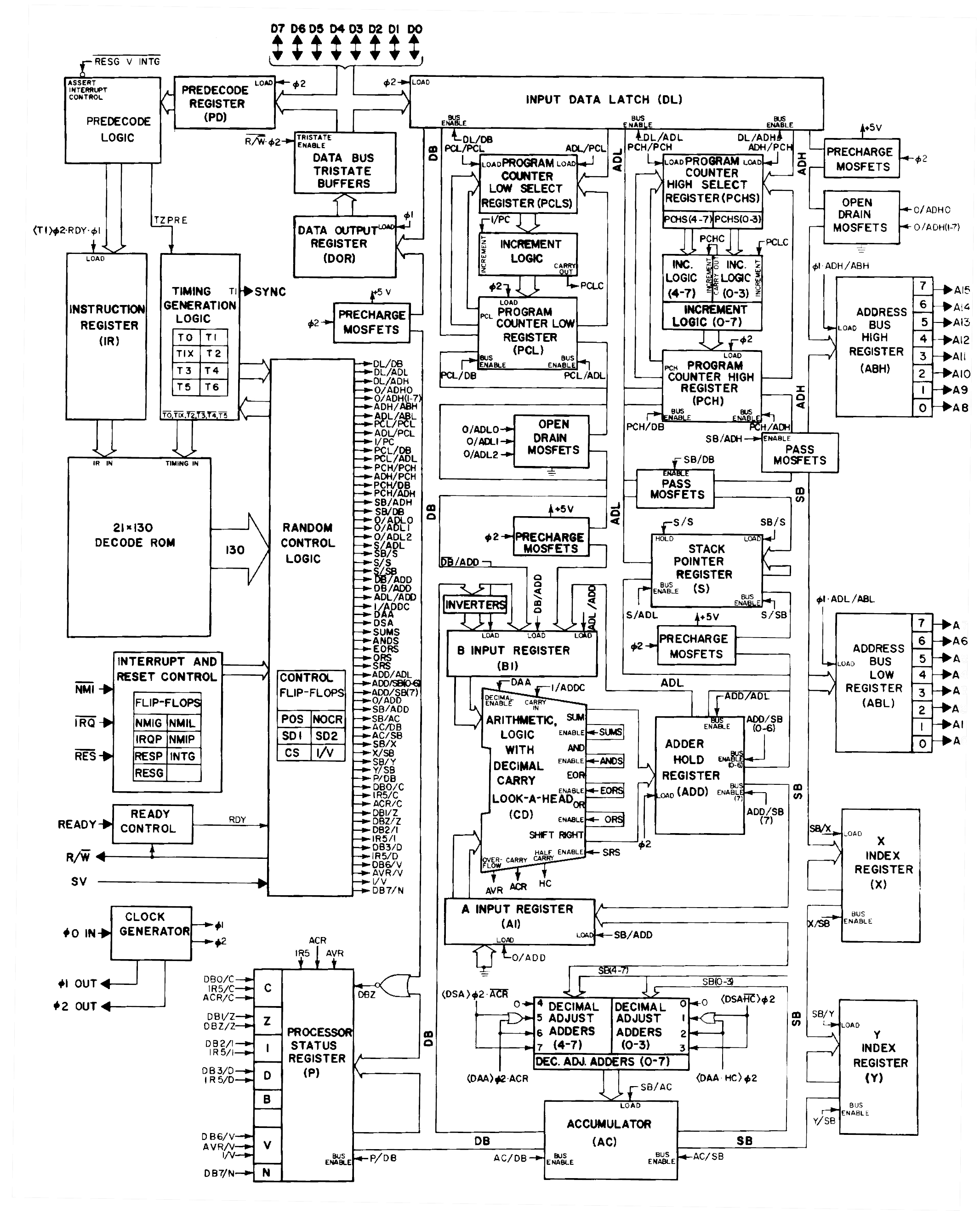
(Original from Apple II things)
The Decode ROM (PLA)
There is no need to understand the whole diagram. The important part is on the left: The instruction register, which holds the opcode, and the current clock cycle within the instruction (T0 to T6) get fed into a 130×21 bit decode ROM, i.e. a ROM with 130 lines of 21 bits each. On the die shot, this is the green area on the bottom.
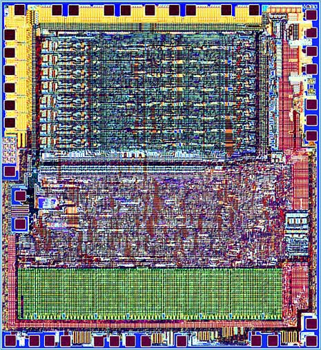
(Original from Molecular Expressions)
While other CPUs from the same era used microcode to interpret the instruction, the 6502 had this 130×21 bit PLA. All lines of the PLA compare the instruction and the current clock cycle, and if they match, the line fires. A little simplified, every line looks like this:
| ON bits | OFF bits | timing | |||||||||||||||||||
| 7 | 6 | 5 | 4 | 3 | 2 | 1 | 0 | 7 | 6 | 5 | 4 | 3 | 2 | 1 | 0 | T6 | T5 | T4 | T3 | T2 | T1 |
(See the diagrams at http://impulzus.sch.bme.hu/6502/ for details; partial English translation of the website here).
- “ON bits” specifies, which bits need to be set for this line to fire.
- “OFF bits” specifies, which bits need to be clear for this line to fire.
The opcode table of the 6502 is laid out in a way that you can find easy rules to generalize the effects of similar opcodes. For example, the branch opcodes are encoded like this:
%aab10000
where “aa” is the condition (00=N, 01=V, 10=C, 11=Z) and “b” decides whether the branch is taken on a set or a clear flag.
So the following line would fire on the first cycle of any branch:
| ON bits | OFF bits | timing | |||||||||||||||||||
| 7 | 6 | 5 | 4 | 3 | 2 | 1 | 0 | 7 | 6 | 5 | 4 | 3 | 2 | 1 | 0 | T6 | T5 | T4 | T3 | T2 | T1 |
| 0 | 0 | 0 | 1 | 0 | 0 | 0 | 0 | 0 | 0 | 0 | 0 | 1 | 1 | 1 | 1 | 0 | 0 | 0 | 0 | 0 | 1 |
From now on, let’s write it differently, so that it’s more readable:
| mask | cycle | description |
| XXX10000 | T1 | T1 of Bcc: fetch branch offset |
If a line fires, it outputs a “1”. The “Random Control Logic” that can seen in the diagram then AND/OR-combines some lines and feeds the result into various components of the CPU: In the case of a branch, this would result in fetching the branch offset, for example.
One line can fire for several opcodes that are similar in their encoding and thus their behavior: For example, “LDA abs”, “ORA abs” and “AND abs” all do the same thing (fetch the low byte of the address) in T1, so there can be a line that matches all these opcodes and causes a memory fetch and a PC increment. Also, multiple lines can fire at the same time for any given cycle within an instruction, which will have the combined effect of the single lines.
LDA and LDX becomes LAX
Now there are many undefined opcodes. The designers of the 6502 have not created any specific PLA lines for them, but since their opcodes are similar to well-defined opcodes, there might be lines that fire nevertheless.
Let’s take opcode $AF for example, which is “LAX absolute”. It loads a value from an absolute address in memory and stores it in A and X at the same time. This is somewhat the combination of opcodes $AD (LDA abs) and $AE (LDX abs).
The instructions “LDA/LDX/LDY abs” ($AC/$AD/$AE) consist of four cycles:
- The first cycle fetches the low byte of the address.
- The second cycle fetches the hgh byte of the address.
- The third cycle fetches the address from memory and stores it in A/X/Y.
- The fourth cycle fetches the next instruction.
Cycles T1, T2 and T4 are identical for all three of them, and they are encoded smilarly, so the following three PLA lines can be used to detect these instructions and signal the rest of the CPU to carry out the specific tasks:
| mask | cycle | description |
| 101011XX | T1 | T1 of $AC/$AD/$AE: fetch addr/lo |
| 101011XX | T2 | T2 of $AC/$AD/$AE: fetch addr/lo |
| 101011XX | T4 | T4 of $AC/$AD/$AE: fetch next opcode |
The mask %101011XX doesn’t only fire for $AC/$AD/$AE, but also for the undefined opcode $AF: So $AF (LAX) behaves the same as LDA/LDX/LDY in T1/T2/T4, i.e. it fetches a 16 bit address and in the end fetches the next opcode.
T3 differs in all three cases, so it has to be handled by one separate line per case:
| mask | cycle | description |
| 10101100 | T3 | T3 of $AC: read into Y |
| 101011X1 | T3 | T3 of $AD: read into A |
| 1010111X | T3 | T3 of $AE: read into X |
(Actually, the lines in the actual PLA might be less specific, i.e. contain more X bits, since there are similar instructions like “ORA absolute” that might share this line.)
The line for $AC is only true for the exact value of $AC, but the $AD and $AE lines have one “don’t care” bit each. The bitfield of $AF, which is %10101111, is true for both masks, so in T3 of $AF, both the $AD and the $AE lines fire.
In T3, LDA/LDX/LDY have in common that they all read from memory and put the result onto the internal “SB” bus. “LDA” also sets the “SB->AC” control line to “1”, which will make the accumulator read its value from SB. Likewise, LDX causes “SB->X” to be “1” and makes X to read from the SB bus, and LDY reads SB into the Y register.
Since both the LDA and the LDX lines fire, both the accumulator and the X register will be sent the command to load their values from the SB bus, so $AF is effectively an LAX: Load Accumulator and X.
The KIL Opcodes
There are many “KIL” opcodes, i.e. opcodes that stop the CPU, so that it can only recover using a RESET, and not even an IRQ or an NMI.
In order to understand this, let’s look at the different states an instruction can be in. After the instruction fetch, the CPU is in cycle T1. It will feed the opcode and the cycle number into the PLA and cause the rest of the CPU to carry out whatever has to be done in this cycle, according to the PLA. Then it will shift the T bitfield left by one, so the T2 line will be “1”, then line T3 and so on. There are seven T lines total, T1 to T7. At the end of each instruction, the PLA causes the T bitfield to reset, so that the next instruction starts with T1=1 again.
But what happens if T does not get reset? This can happen if in all seven states of T, no line fires that actually belongs to an instruction that ends at this cycle. T gets shifted left until state T7, in which another shift left will just shift the 1 bit out of T – all bits of T will be zero then, so no PLA line can fire any more.
All interrupt and NMI requests are always delayed until the current instruction is finished, i.e. until T gets reset. But since T never gets reset, all interrupts and NMIs are effectively disabled.
What’s next?
There are many illegal opcodes, some with very weird behavior, and some that have been documented as unstable. Studying all these can reveal many interesting details about the internal design of the 6502.
Cool stuff! I remember the illegal ops from The Old Daysâ˘, this explanation is excellent
I remember programming the 6502 in machine language on my Ohio Scientific C24P … man that was a long time ago! Heck, can you even buy a 6502 any more? It was a heck of a chip. I also liked the 68hc11.
> Heck, can you even buy a 6502 any more?
You sure can! Western Design Center still manufactures and sells the CMOS 65c02 and the 16-bit 65c816: http://www.westerndesigncenter.com/wdc/w65c02s-chip.cfm
I was a wuss and never dared use those opcodes in production code. I never thought it was safe to rely on them remaining the same in later revisions of the chip…I see I may have been wrong..
Actually, the 65Cxxxx series proved you right. 65C02 and 65C816 most definitely didn’t support most of them. Now, if you had been using a known non-“C” chip, then you could have happily kept using them. The NES for example, never changed the instruction set, even though part of the vetting process was to ban illegal opcodes in application code (i.e. games). Anything that came with the CPU as an integreated part didn’t matter though, since you’d just ship out the compatible firmware in soldered mask ROM’s. 😉
You can keep guessing prompt formulas. Or you can open AIPromy, click “Viral Prompts”, and get what’s already working today.
You are over 20 year late on this news…just like lots of things on the internet these days. I remember the undocumented instructions being documented and published back in the 80’s.
I don’t think he’s breaking the news, he’s explaining how the decode system wound up making them exist in the first place.
I programmed the 6502 cousin chip, the 6507, for Atari 2600 games in the 1980’s. We discussed using undocumented opcodes but felt any benefit discovered would be exceeded by the risk that the CPU mask might be updated, ‘fixing’ the undocumented ‘feature’, and our games may not work.
Now the graphics chip in the Atari 2600, that was a different story. We were willing to bit bang different registers to achieve ‘impossible’ graphics, like extra sprites on a raster. Those who had to reverse engineer Atari 2600 had an advantage over Atari employees. We weren’t given a manual telling us how the chip worked, we had to do trial and error to learn the inner workings and see what was really possible.
Amazing. Would you still have details on that?
I did lots of 6502 assembly language programming on my old OSI Challenger 1P and later I did some on an Apple II. I remember some of those illegal opcodes we referred to as HCF (Halt & Catch Fire), probably the ones you refer to as KIL.
We used illegal opcodes and a piggy-back board to add instructions to the 6502 processor. When we decoded an illegal opcode, we floated a no-op onto the instruction bus (for a defined number of cycles) and then let our custom PAL decode what really should happen. Doing this, we added a “paging register” for the zero-page and 1xx page (which you know are special). For the 1xx page, we detected when stack overflows and underflows happened and auto-adjusted the 1xx page register. Doing this gave us a 256-byte window into a (essentially) 64K stack. This was instrumental in the Forth interpreter we used to control a custom radar dish (details not available, sorry). We also took advantage of the fact that the 6502 was a DC-clock-safe processor , and essentially stopped the clock while slower RAM was being accessed and over-clocked the processor when it was talking to zero-page stuff. Lots of memories there. BTW, this was 1979-1982 or so…
Hello Marc,
It’s been a while since you posted this message.
But I’m very curious how you did this. Can you give me some more details?
In 1980 the Computhink Minimax was released.
It has a “hybrid” CPU that’s 6502 compatible and has 64 user definable microcode instructions. There’s almost no information on this machine.
Do you know if they used the same trick as you did?
Is there any production code that used the behaviour of the illegal opcodes? I imagine these will pose a challenge to modern-day 6502 emulators…
@bi: I remember a disk copy program on the C64 that used an illegal opcode to save 2 cycles in a transfer routine for the serial bus.
@bi: I bet most of the more sophisticated (game) copy protections used illegal opcodes to make cracker’s work as hard as possible, amongst other tricks.
Very interesting. Is a dump of the 130×21 decode rom available?
I read on Wikipedia that some Apple II games actually used illegal opcodes, and they failed to work right when the illegal opcodes were ‘fixed’ for the Apple IIc
http://en.wikipedia.org/wiki/Illegal_opcode
@bi: There are some programs out there which actually use the illegal opcodes. “In general”, they do not pose big challenges to 6502 emulators, as most (all?) of them are emulated correctly – at least, to the extent they are acutally documented. However, there are always people telling that the implementations are not correct, as “their” 6502 behaves differently. Perhaps, there were really small variations to the mask?s
@ed: Later versions of the 6502 (for example, the CMOS version 65C02) did indeed change the illegal opcodes or added other opcodes (i.e., 65816). Thus – as always – it was a much better bet to stay on the safe side and only use documented features.
– Spiro
“Anybody who would spend considerable effort emulating a C64 is not
particularly sane to begin with; it is unreasonable to expect them to
produce sane software.”
(“asuffield” in http://forums.thedailywtf.com/forums/p/7199/134136.aspx)
This is good stuff. As a die-hard 6502-coder from my VIC20 days in the early 80s right through to now, it’s always nice to see new information being added to the body of knowledge about this kick-ass little chip. Although the ‘undocumented’ instructions have been known about forever, and indeed the speculation that they were a result of crosstalk in the decode PLA has always been the likliest cause, I don’t recall reading anything before about how the decode logic actually sequences the instruction based on the T-state counter and uses that as a lookup into the PLA.
Question: is the T-state shifter locked to the master PHI clock? Or can several T-states execute ‘below the radar’ independently of physical clock cycles?
Although there are a lot of 6502 emulators out there, and a fair few machine emulators that recreate those 8-bit micros based upon the 6502, my project is to emulate the chip at the hardware level (i.e. mimic not just the activity of the documented opcodes, but also properly replicate the undocumented ones as well). The way I’m doing it is to essentially design an interpreted microcode that describes the action of the chip at the physical level, and thus extends to the instructions themselves – all 256 of them, useful or not. 😉 The idea is to finish with a cycle-perfect, behaviour-perfect emulation that accurately reproduces the function of the hardware, right up to and including anomalies like the LAX instruction (to name but one) and the indirect JMP page boundary bug.
The project has been running in my spare time for about a year, and is at the stage of a functioning chip but needs refinement – all the logic for the undocumented opcodes has been gleaned from a massive amount of research and collation of information from where-ever the term ‘6502’ has popped up in a search result!
This little article has given me a new insight into the way the 6502 works at the lowest level, and has prompted an idea or two. What would be REALLY useful is a full expansion of your PLA bitpattern table for all instructions / addressing modes / T-states – this would pretty-much replace my derived behaviour decision tree with a ‘real’ replica of the actual hardware table. Pretty please? 😉
As a “modern” 2600 programmer, I make use of the undefined opcodes when applicable; LAX and SAX are quite common; DCP is handy. I use different the zp and abs addressing modes of NOP as a matter of course to hit address strobes, though CMP or BIT would in most cases work as well (depending whether C or V is important).
I’d like to know more about the state machine. Since there are only six ‘t’ inputs shown, but instructions can take up to eight clocks, it would seem the encoder can’t be a “one-hot”, but I’m not sure what the actual sequence would be. Certainly it would make sense for the third through fifth cycles of “DCP zp” to execute the same state sequence as the sixth through eighth of “DCP (zp),y”.
I’m also curious how the chip’s design came about historically. There are an amazing number of irregularities in the instruction set, despite the fact that all of the instructions could be placed in easy and regular fashion:
1qqqqmmm — ADD,ADC,BIT,SBC, AND,ORA,EOR,CMP, LDA,STA,LDX,STX,LDY,STY,CPX,CPY
All with eight addressing modes (incl. immediate)
01qqqmmm — INC,DEC,ASL,ROL,LSR,ROR,JMP,JPI
All with eight addressing modes (incl. accumulator)
00qqqqqq — Everything else
Room for all the existing multi-mode instructions, plus ADD (I’m regarding Jump-Indirect as a separate instruction from JMP)
While some addressing modes might not have worked with some instructions, I would think laying out the opcode map as indicated above would have been much simpler than having different sets of addressing modes for different instructions. Any idea how the actual arrangement came about?
@supercat: According to the block diagram there are eight states – T0, T1, T1X, T2, T3, T4, T5, & T6.
If the PLA width is 21, then excluding the two 8-bit masks leaves us with only 5 bits. How do they map to the 8 possible clocks per instruction or the T0..T6 numbering?
Vladitx: The schematic shows that the PLA is actually 22×137, so there are 6 bits for timing. Guesses: The first cycle is identical for all instructions, so it wouldn’t need to go to the PLA at all. Then there’s T1X, which could be the extra cycle added for indexed address operations. That does mostly the same thing as T1. I imagine T1 would be active for two cycles in that case, with the differences dealt with separately.
MagerValp: http://impulzus.sch.bme.hu/6502/letolt.php3 has large postscript files with the transistor-level schematic. The PLA is very obvious, at the bottom. If I can find the enthusiasm, I’ll print it out and try to confirm my guesses.
Enlighenment: You didn’t read the article. The undocumented instructions have been known for ages, yes. That point was made in the second paragraph. That was done by executing each instruction and seeing what happened. What’s new is reverse-engineering from the actual chip. This is not “what they do”, but “how they do it”. We didn’t have those beautiful micrographic pictures in the 80s.
Yes, I’ve seen the schematics, but translating it into a bit array is beyond my capabilities.
OK. First I need to learn to count. There are indeed 21 rows in the PLA. There are still 6 from the timing block: the missing one is from bit 1 of the instruction. That bit can be 1 or don’t care. There’s no way to require it to be 0 (unless I’ve got my zeroes and ones swapped). That’s interesting.
There could also be 130 columns. The schematic has 137, but a few are unused.
I’ve transcribed the PLA from the schematic, and put it at http://www.ucc.gu.uwa.edu.au/~john/6502/pla.txt
Until I work out what the signals from the timing block are, I’ve called them A-F. – means there’s no connection (which could mean this signal is active for all cycles if the instruction matches, or there’s an error in the schematic). The last part of each line specifies which instructions match. 0 for 0, 1 for 1, x for don’t care.
So the second line (labelled “2”) is active on clock cycle D whenever the instruction matches xxx100x1: $11, $13, $31, $33, $51, $53, …
What these outputs do is another matter.
There are likely to be errors in my transcription, and there are probably errors in the schematic too. The photo isn’t easy to interpret, and there are some large bits of dust blocking some of the PLA. My attempt at reading the first few columns gives me something that looks nothing like any part of the schematic.
But this is fun, so I won’t give up yet.
John: ok, now we’re getting somewhere 🙂 Figuring out what each rule does should be easy once the timing signals are mapped out. The multitude of xxxxxxxx lines makes me wonder though…
John,
I’ve double checked your pla.txt file against the schematic. I think lines 43, 44, and 45 should read:
43: E xxx100x1
44: C xxx100x1
45: D xxx11xxx
You had leading zeros instead of the three X’s
The home computer emulators for Linux and PC (eg. atari800) simulate the entire operation of a 6502 system right down to the audio and video coprocessors. The authors have a complete list of all the illegal opcodes in order to ensure compatibility with all the assembly language games written at that time.
Like Marc Brooks (above), I too used hardware to detect illegal opcodes and thereby add new instructions to a 6502 processor. In my case the features included a 16 MB address space and a very fast, one-byte Forth NEXT instruction. There’s a full description here
http://www.laughtonelectronics.com/arcana/BrideOfSonPg1.html
and a Forum discussion here
http://forum.6502.org/viewtopic.php?t=1487&postdays=0&postorder=asc&start=0
Was inspired to look into the HCF opcodes when someone posted me a Javascript transistor-level 6502 simulator – http://visual6502.org/JSSim/index.html … had been wondering whether this simulator would run these illegal opcodes … if it’s a good enough simulator it should … 🙂
A fascinating article. It leads to the next question, what else can we say about the behavior of the status register as a register? For example, is there anyhing interesting about the unasigned bits? Internally it’s undoubtedly a bunch of separate control signals that are only treated as a complete byte on pushes/pops.
The Apple II+ was our family’s first computer and got me on track towards a computer science degree. The predictability of the hardware and software made learning rewarding, and allowed people to push the system to an amazing degree.
@john, @ed, @strick – I came across this exact problem. The early BBC computers (e.g. the BBC B) used the 6502, whereas later ones like the BBC Master used the 65C02. This resulted in a bunch of games having to be rewritten for the BBC Master.
Just in case it saves anyone the confusion I just experienced:
The PLA columns are presumably pre-charged on Phi2, and then any active connected row will discharge the column on Phi1.
Many games made good use of the Illegal opcodes as did games protection.
For Marc Brooks above (a little OT): Are you sure you were ever overflowing the stack? In Forth which is explicitly stack-oriented and everything goes through the stacks, my tests showed that maximum usage of each of the two stacks (page-1 and ZP) was less than 20% of the page when running a main job in the background while compiling, assembling, and interpreting in the foreground while servicing the input stream interrupts in high-level Forth, plus running the RTC on NMI. Basically that’s like four tasks at once, which combined, took less than 20% of the page-1 return stack space (which also holds stuff for compiling and running program structures, as well as sometimes temporary data storage) and the same for the data stack in ZP. If you do the tests, I think you’ll find you aren’t using nearly as much stack space as you’re afraid you are.
Further to Garth’s question (above):
Marc Brooks’ radar controller using illegal 6502 instructions is described in more detail here: http://forum.6502.org/viewtopic.php?f=4&t=2173
Also, my own “illegal” 6502 instruction-set expansion has a new, abbreviated description here: http://laughtonelectronics.com/arcana/Kimklone_short_summary.html
BTW, right after “every line looks like this:” the table was pretty confusing at first because it looked it every bit was both on and off at the same time.
One more article for your collection (written when I was 18, published in Compute! magazine): https://www.atarimagazines.com/compute/issue41/Extra_Instructions.php
Great insights. I’ve been exploring AI podcast tools like turbocast lately—it’s amazing how quickly content can be turned into audio now.
Stuck on a creative block? nanobanana2
can help you break through.
Really interesting perspective. I’ve been exploring astrocartography tools like AstroChart lately, and it’s fascinating how location can influence different aspects of life.
Really interesting perspective.
Searching for a Massage spa near me? Finding a clean, comfortable, and relaxing place can make all the difference. Enjoy a peaceful atmosphere and quality massage experience to help you relax and feel refreshed after a long day.
This deep dive into MOS 6502 illegal opcodes is absolutely masterful! I’ve read countless articles documenting what these opcodes do, but your explanation of *why* they work at the PLA level is genuinely unprecedented. The way you traced how the decode ROM masks for LDA/LDX/LDY accidentally overlap to create LAX is such an elegant revelation — it turns “undefined behavior” into perfectly logical hardware behavior. The KIL opcode explanation through the T-state shift mechanism is equally brilliant.
I’ve been getting into casual browser games lately while reading through your reverse-engineering posts and running emulation tests. Head Football has become my go-to — it’s this simple physics-based soccer game that’s surprisingly addictive for quick breaks. My retro computing friends and I compete for high scores during our virtual 6502 assembly sessions, and it’s become a fun way to reset between intense debugging of old NES code. The matches are short enough that I never miss a breakpoint or a cycle-count discrepancy!
Your work on visual6502 and these PLA analyses is preserving computing history in the most rigorous way possible. Thanks for another absolutely essential read — Page Table remains the gold standard for CPU archaeology.